Quantifying Interfacial Intermetallic Growth Kinetics and Failure Mechanisms under High Temperature Thermal Aging
Quantifying interfacial intermetallic growth kinetics under thermal aging enables accurate interconnect lifetime predictions and prevents field failures.


Thermodynamics
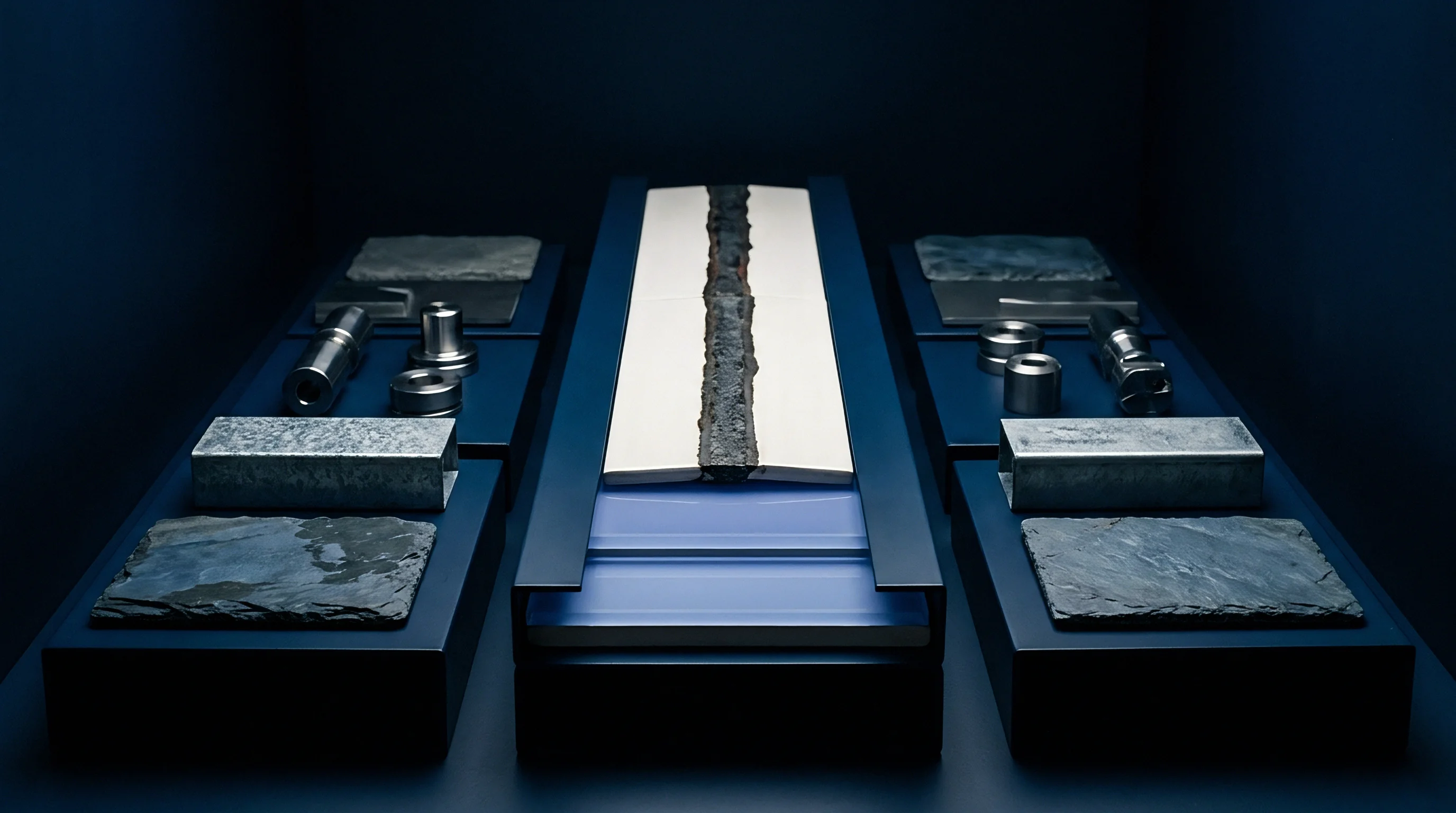
Solid State Rate Equations
At elevated operating temperatures, solid-state interdiffusion across metallic interfaces drives continuous phase growth governed by Fickian transport principles. When volume diffusion through the growing compound controls the reaction, interfacial layer growth during thermal aging follows a parabolic rate law. The total thickness of the interfacial compound layer, denoted as x(t), at time t under an isothermal aging temperature T, follows a non-linear relationship expressed as:
x(t) = x_0 + (k_v t)^n
Here, x_0 is the initial phase thickness resulting from the reflow profile. The symbol k_v denotes the growth rate coefficient at temperature T, and n represents the time exponent. When grain boundary diffusion or interfacial reactions dominate, n deviates from the classic parabolic value of 0.5 ~ shifting toward 0.33 for grain-boundary mechanisms or 1.0 for reaction-rate limited regimes.
In copper-tin systems involving lead-free alloys such as SAC305 (Sn-3.0Ag-0.5Cu), two primary equilibrium phases form at the substrate junction: the epsilon phase (Cu3Sn) adjacent to the copper substrate and the eta phase (Cu6Sn5) adjacent to the bulk solder matrix.
The temperature dependence of the growth rate coefficient k_v follows an Arrhenius relationship:
k_v = k_0 exp(-Q / (R T))
In this expression, k_0 represents the pre-exponential frequency factor, Q signifies the apparent activation energy in Joules per mole, R stands for the universal gas constant (8.314 J/mol·K), and T represents the absolute thermal aging temperature in Kelvin. Determining these kinetic constants requires multi-temperature aging regimes, typically executed across a thermal spectrum of 125°C, 150°C, and 175°C, with duration intervals extending from 100 hours to 2000 hours.
This kinetic divergence appears in lead-free solder interconnects during qualification. An Arrhenius plot of the natural logarithm of k_v against reciprocal absolute temperature (1/T) yields a straight line with a slope defining -Q/R. Experimental evaluations across Sn-Pb, SAC305, and nickel-plated systems reveal distinct activation energy barriers that govern phase layer growth rates over extended field operational lifetimes.

Phase Sequence at Bimetallic Boundaries
Interfacial transport mechanics alter the chemical makeup of the bond line as thermal aging proceeds. In pure copper and tin couples, Cu6Sn5 forms immediately during reflow solidification. Sub-solidus thermal storage triggers the nucleation of Cu3Sn between the original copper pad and the Cu6Sn5 layer.
The thermodynamic driving force stems from the chemical potential gradient across the system: tin atoms diffuse rapidly down the concentration gradient toward the copper interface, while copper atoms migrate outward into the solder matrix.
| Interface Couple | Dominant Phase | Activation Energy Q (kJ/mol) | Pre-exponential k_0 (m²/s) | Temperature Range (°C) |
|---|---|---|---|---|
| Cu / SAC305 | Cu6Sn5 + Cu3Sn | 84.5 | 3.2 10^-7 | 100 – 175 |
| Cu / Sn-37Pb | Cu6Sn5 + Cu3Sn | 78.2 | 1.8 10^-7 | 100 – 150 |
| Ni(P) / SAC305 | (Ni,Cu)3Sn4 | 105.3 | 8.6 10^-6 | 125 – 175 |
| Cu / Al Bond Wire | CuAl2 / Cu9Al4 | 112.1 | 1.4 10^-5 | 150 – 200 |
When electroless nickel immersion gold (ENIG) or electroless nickel electroless palladium immersion gold (ENEPIG) surface finishes serve as the substrate barrier, the reaction sequence shifts. The nickel layer acts as a diffusion barrier, slowing copper transport while the interface forms Ni3Sn4 or ternary (Ni,Cu)6Sn5 phases. As thermal exposure continues, nickel dissolves into the solder, generating a phosphorus-rich layer (Ni3P) directly behind the intermetallic layer.
High localized tensile stress and low fracture toughness make this nickel-phosphorus layer inherently unstable.
The activation energy for Cu3Sn phase growth in SAC305 interconnects sits at 84.5 kJ/mol under isothermal aging between 125°C and 175°C.
Total growth rate scales non-linearly with dwell duration. In wire bonding systems using copper wire on aluminum bond pads, thermal aging above 150°C induces continuous interdiffusion, yielding a series of copper-aluminum phases: CuAl2 (theta phase), CuAl (eta phase), Cu4Al3 (zeta phase), and Cu9Al4 (gamma phase). Each phase exhibits unique lattice parameters, elastic moduli, and thermal expansion coefficients.
Accumulation of these brittle intermetallic layers alters local stress states, accelerating failure during subsequent thermomechanical cycling.
Initial cross-sectional imagery taken right after reflow does not demonstrate long-term joint integrity, as solid-state diffusion during thermal aging reorganizes the interface regardless of initial bonding clarity.


Grain
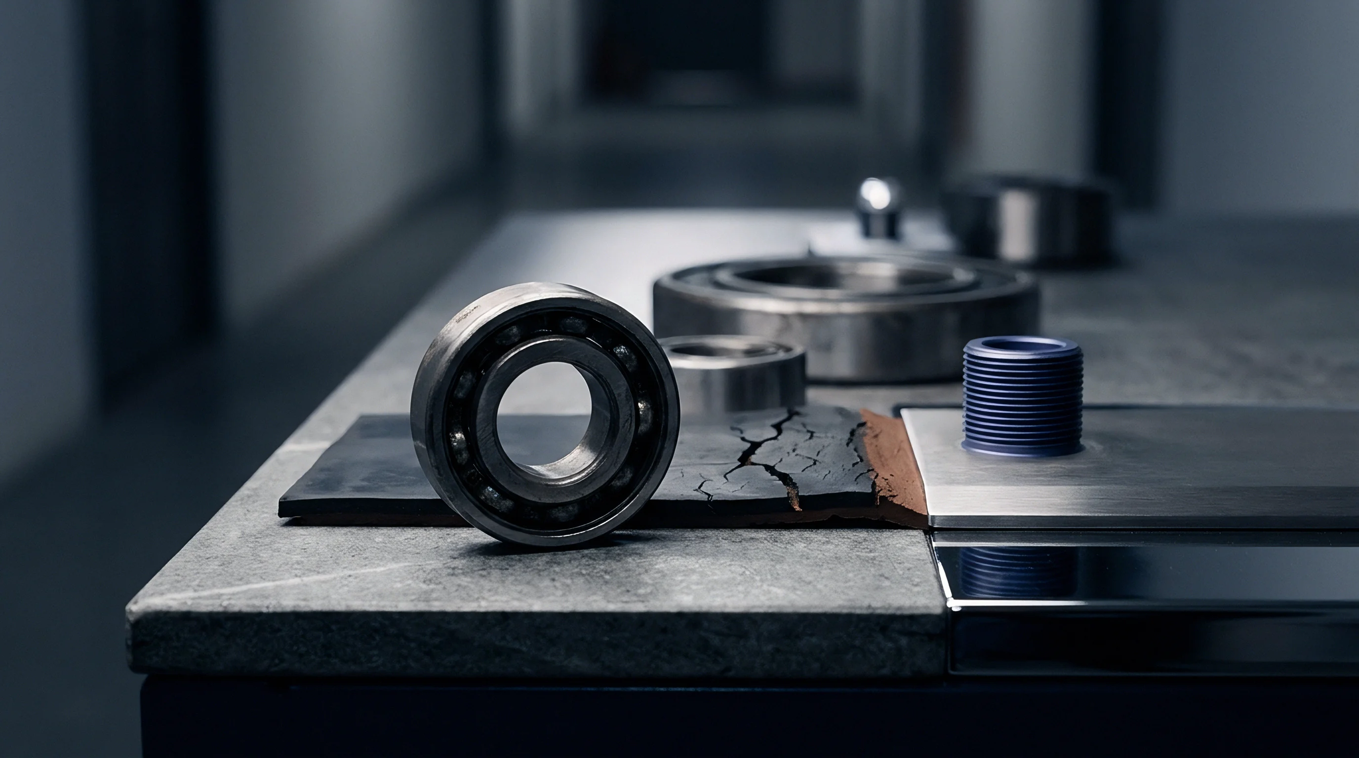
Microstructural Evolution and Coarsening
Morphological stability within the interfacial layer declines as thermal aging progresses. Initial intermetallic structures formed during reflow show scallop-like geometries driven by liquid-solid dissolution kinetics. During high-temperature storage, solid-state diffusion flattens these scallops into a planar morphology to reduce total interfacial free energy.
Grain boundaries within the Cu6Sn5 layer coarsen significantly, reducing total grain boundary surface area per unit volume.
Sub-micron grains observed in the as-soldered state grow into multi-micron domains after 500 hours at 150°C. This coarsening decreases grain boundary diffusion paths, shifting the dominant mechanism toward bulk volume diffusion. Volume transport requires higher energy input, slowing the linear accumulation of phase thickness over long durations while increasing intrinsic lattice strain within individual grains.
Phase Failure Modes
Brittle interfacial failure modes originate from microstructural changes occurring inside the compound layers during extended thermal aging. Tensile stresses build up due to density mismatches between parent metals and the resulting compound phases. For instance, converting Cu and Cu6Sn5 into Cu3Sn involves a molar volume contraction of approximately 5 percent, introducing localized tensile stresses directly at the Cu3Sn/Cu boundary.
- Interfacial Micro-cracking forms along the planar interface between Cu3Sn and copper pads due to volumetric shrinkage during phase transformation.
- Void Coalescence occurs as atomic vacancies aggregate along grain boundary junctions within the Ni3P layer on ENIG surfaces.
- Phase De-lamination occurs when thermal expansion mismatches between bulk compound phases induce shear fractures under mechanical shock.
- Solder Matrix Depletion develops as tin atoms are consumed from the adjacent solder matrix, leaving behind solute-rich, low-ductility phases.
A planarized intermetallic interface concentrates mechanical shear stress far more effectively than an un-aged scallop morphology.
High thermal exposure alters anisotropic crystal orientations: hexagonal Cu6Sn5 transforms into a monoclinic structure when cooled below 186°C, creating internal micro-strains that weaken the mechanical strength of the interconnect.
Intermetallic growth consumes substrate copper, reducing the effective load-bearing area of the original pad and predisposing the assembly to brittle fracture under shock loading.


Cavitation
Kirkendall Void Nucleation Mechanics
Vacancy condensation at bimetallic boundaries causes structural degradation in thermal aging environments. Kirkendall voiding occurs when unequal intrinsic diffusion fluxes exist between two interdiffusing species. In the copper-tin system, copper atoms diffuse outward into the Cu3Sn phase faster than tin atoms migrate inward toward the copper substrate.
To maintain structural equilibrium, an excess flux of atomic vacancies flows opposite the fastest diffusing species, moving directly toward the Cu/Cu3Sn interface.
When vacancy supersaturation passes a critical thermodynamic threshold, vacancies nucleate into micro-cavities. Impurities in the electroplated copper pad ~ such as sulfur, carbon, chlorine, and organic brightener residues from electroplating baths ~ lower the free energy barrier for void nucleation. These micro-cavities gather along the Cu/Cu3Sn interface, forming continuous vacancy chains that drastically reduce the fracture energy of the junction.

Quantification of Interfacial Degradation
Assessing void density requires systematic cross-sectional analysis using Field Emission Scanning Electron Microscopy (FE-SEM) combined with Focused Ion Beam (FIB) milling. Quantitative analysis measures two parameters: areal void fraction (percentage of interfacial length occupied by voids) and average void diameter. Micro-cavities initially appear as isolated pores with diameters ranging from 50 to 200 nanometers.
Prolonged thermal exposure at 150°C for 1000 hours causes these pores to coalesce into continuous micro-fissures exceeding 1 micrometer in width.
Continuous Kirkendall voiding drops the high-speed drop-impact strength of lead-free solder joints by up to 80 percent, even when low-speed lap shear test metrics show minimal degradation.
Executing an accelerated thermal aging qualification routine requires a controlled testing protocol:
- Select sixty test coupons from three independent substrate plating batches to account for bath chemistry variations.
- Perform cross-sectional scanning electron microscopy on five baseline specimens to record initial phase thickness and baseline void density.
- Place the remaining fifty-five specimens in an isothermal environmental chamber maintained at 150°C with continuous temperature logging.
- Extract ten specimens at discrete time intervals of 100, 250, 500, 750, and 1000 hours.
- Prepare polished cross-sections using argon ion polishing to avoid mechanical smearing of nanometer-scale cavities.
- Measure total intermetallic layer thickness and count Kirkendall void area fraction across ten standardized fields of view per sample at 10,000x magnification.
- Subject the remaining specimens to high-speed ball shear testing at a shear speed of 1.0 meter per second to determine ductile-to-brittle failure mode transitions.
| Aging Time (Hours) | Total IMC Thickness (µm) | Cu3Sn Layer Thickness (µm) | Kirkendall Void Area Fraction (%) | Brittle Fracture Mode Ratio (%) |
|---|---|---|---|---|
| 0 (As-Reflowed) | 1.25 | 0.10 | 0.0 | 0.0 |
| 100 | 2.10 | 0.45 | 0.8 | 5.0 |
| 250 | 3.15 | 0.85 | 2.3 | 18.0 |
| 500 | 4.40 | 1.40 | 6.5 | 52.0 |
| 750 | 5.30 | 1.95 | 11.2 | 81.0 |
| 1000 | 6.10 | 2.40 | 16.8 | 98.0 |
Mechanical performance declines sharply as brittle phase thickness grows. Standard-speed shear strength testing (0.1 mm/s) shows a gradual decrease in peak load, whereas high-speed testing reveals a rapid transition from ductile bulk shear to brittle interfacial cleavage. This shift occurs once total intermetallic thickness exceeds 4 micrometers or when the Kirkendall void area fraction along the Cu3Sn interface passes 5 percent.
Ignoring substrate plating bath purity metrics leads to catastrophic field returns caused by accelerated Kirkendall voiding under normal thermal aging conditions.


Metrology
Analytical Characterization Techniques
Accurate measurement of interfacial compound layers requires precise analytical procedures. Standard optical microscopy lacks the spatial resolution needed to resolve sub-micron phase boundaries, such as the thin Cu3Sn layer in as-soldered joints or the phosphorus-rich layer in ENIG finishes. Scanning Electron Microscopy (SEM) operated in backscattered electron (BSE) mode provides atomic-number contrast, differentiating Cu6Sn5 from Cu3Sn and substrate copper.
Energy Dispersive X-ray Spectroscopy (EDS) line scans and elemental mapping quantify phase stoichiometry. Transmission Electron Microscopy (TEM) combined with Focused Ion Beam (FIB) sample preparation enables atomic-scale resolution of early-stage phase nucleation and lattice defect structures. Nanoindentation measures localized mechanical properties across thin interfacial phases, outputting elastic modulus and hardness values for individual compound layers.

Does Accelerated High Temperature Aging Predict Field Lifetime?
Relating high-temperature laboratory test results to operational field life relies on kinetic modeling grounded in Arrhenius parameters. Qualification protocols employ High Temperature Storage (HTS) standards such as JESD22-A103 to simulate field thermal exposure. Testing at elevated temperatures (125°C to 175°C) accelerates solid-state atomic transport, compressing years of operational stress into weeks of laboratory testing.
Applying thermal stress carries risks if aging temperatures exceed phase transformation limits or melting points of eutectic microstructures. Aging lead-free solders above 175°C alters the dominant diffusion mechanism, yielding inaccurate activation energies that distort operational lifetime estimates. Valid kinetic extrapolation demands testing across at least three distinct temperatures below structural phase change thresholds.
Selection of analytical instrumentation relies on clear operational metrics:
- SEM Backscattered Imaging differentiates intermediate phases based on mean atomic number variations.
- Focused Ion Beam Sectioning eliminates mechanical smearing artifacts during void analysis along fragile boundaries.
- X-ray Diffraction Spectroscopy determines crystal structure orientation and tracks phase transformations across thermal cycles.
- High-Speed Impact Shear Testing measures brittle fracture resistance under stress states that match real-world drop events.
A qualification protocol that relies solely on room-temperature shear strength tests fails to detect interfacial brittle embrittlement induced by thermal aging.
Reliability models combine empirical parabolic rate constants with finite element analysis (FEA) to calculate stress distribution across thermal regimes.
Standard purchase specifications must specify IPC-TM-650 Method 2.1.1 for microsectioning and set a limit of maximum 10 percent Kirkendall void length fraction along the load-bearing interface after 500 hours at 150°C.

Fatigue

Thermomechanical Interaction with Aged Interfaces
Thermal aging combined with cyclic thermomechanical loading accelerates joint failure. In field applications, printed circuit board assemblies endure power cycling and ambient temperature changes. Thermal expansion mismatches between electronic components and organic substrates generate cyclic shear strains across interconnects.
When an assembly undergoes thermal aging, the interfacial compound layer thickens while the bulk solder matrix softens through grain coarsening and strain recovery.
This microstructural separation concentrates applied shear strain directly at the rigid, non-yielding intermetallic layer. The brittle compound layer cannot deform plastically to accommodate strain, driving crack initiation and propagation along phase boundaries. Thermal aging shifts the primary crack path from the bulk solder matrix directly to the interfacial compound layers.
| Material / Phase | Elastic Modulus E (GPa) | Hardness H (GPa) | Coefficient of Thermal Expansion (ppm/°C) | Fracture Toughness K_1c (MPa·m^0.5) |
|---|---|---|---|---|
| Bulk SAC305 Solder | 51.0 | 0.15 | 20.0 | 1.8 – 2.2 |
| Cu6Sn5 (Eta Phase) | 85.5 | 6.20 | 16.3 | 1.4 |
| Cu3Sn (Epsilon Phase) | 108.3 | 7.40 | 19.0 | 1.2 |
| Ni3Sn4 Phase | 133.0 | 8.10 | 13.7 | 1.1 |
| Copper Substrate Pad | 121.0 | 1.10 | 16.5 | 30.0 + |
High local elastic modulus discrepancies between Cu3Sn (108.3 GPa) and bulk SAC305 solder (51.0 GPa) exacerbate stress concentration factors. Cyclic thermal shock testing (per JESD22-A104, Condition G: -40°C to 125°C) applied after high-temperature aging causes rapid crack propagation through pre-existing Kirkendall void networks.
Preventing premature fatigue failures requires strict control over interconnect metallization parameters:
- Enforce Substrate Plating Purity by restricting organic brightener content in copper electroplating baths to suppress Kirkendall void formation during thermal aging.
- Specify Barrier Layer Thickness ensuring electroless nickel layers maintain a minimum thickness of 3.0 micrometers to block copper out-diffusion.
- Optimize Reflow Peak Temperature keeping peak temperatures below 245°C to limit initial intermetallic layer thickness to under 1.5 micrometers.
- Incorporate Micro-alloying Additives such as cobalt, nickel, or bismuth into lead-free solder matrices to slow intermetallic phase growth kinetics.
Thermomechanical cycling reduces component operating life once the intermetallic layer thickness exceeds 5 micrometers. Combined environmental testing ~ applying thermal aging before temperature cycling ~ yields more realistic data for field reliability predictions.
The key unresolved issue centers on how multi-axial stress fields alter atomic diffusion rates within sub-micron intermetallic layers during simultaneous vibration and thermal exposure.

Risk

Commercial Liability and Financial Impact
Interfacial degradation caused by high-temperature aging poses commercial risks for high-reliability applications in automotive, aerospace, and industrial control sectors. Interconnect failures in field environments trigger recall expenses, warranty liabilities, and legal exposures. A failure in an automotive electronic control unit operating in a high-temperature engine bay can lead to systemic vehicle shutdowns.
Mitigating financial risk requires aligning engineering specifications with rigorous quality control protocols. Relying on baseline component supplier datasheets without conducting independent, long-term thermal aging qualification creates significant commercial exposure. Uncontrolled changes in substrate plating chemistry or solder paste formulation can alter intermetallic growth rates, turning a qualified assembly into a high-risk liability.

Supplier Quality Management and Audit Protocols
Contractual agreements must include clear technical thresholds governing interfacial microstructures. Technical clauses should define maximum acceptable intermetallic layer thicknesses and void area fractions after accelerated aging. Audits must inspect substrate plating line bath maintenance records, chemical analysis logs, and cross-sectional testing metrics.
Suppliers must submit microstructural verification dossiers for every change in plating chemistry, base substrate material, or reflow thermal profile. Implementing incoming lot acceptance sampling using accelerated thermal aging tests catches bath contamination issues before components are assembled into finished products.
Quantifying interfacial intermetallic growth kinetics provides the operational baseline needed to enforce quality standards across cross-border manufacturing networks. Coupling clear rate equations with microscopic verification protocols mitigates technical and commercial risks, ensuring long-term product reliability across demanding thermal environments.