Managing Kirkendall Microvoiding and Fracture Risks in High-Density Reflow
Manage Kirkendall voiding by capping plating bath sulfur impurities under 10 ppm and clamping reflow time above liquidus strictly between 45 and 60 seconds.

Physics
Cross-sectional electron microscopy of failed lead-free solder joints reveals microscopic cavity lines running parallel to the substrate contact pad. In high-density reflow operations using SAC305 or SAC105 alloys, solid-state interdiffusion between refined copper pads and molten tin forms distinct intermetallic compound layers. An epsilon-phase intermetallic grows next to the copper base, while an eta-phase layer interfaces with the bulk solder matrix.
Atomic movement across this boundary occurs at unequal rates, as copper atoms migrate into the growing intermetallic much faster than tin diffuses back toward the copper substrate.
This imbalanced atomic flux moves matter away from the copper pad surface. Under classical Fickian diffusion dynamics, an unbalanced flux creates an equivalent counter-flux of lattice vacancies. As heat flows into the joint during reflow, these vacancies migrate toward the interface between the base copper and the epsilon-phase layer.
Once local vacancy concentrations pass thermodynamic equilibrium, supersaturation sets in, and vacancies coalesce into spherical microvoids between 100 nanometers and over 1 micrometer across.
Solder joints exposed to a 150°C thermal aging regime for 500 hours show a microvoid linear density exceeding 25 voids per 100 micrometers along the Cu3Sn interface.
High peak reflow temperatures speed up vacancy generation, and repeated thermal cycles ~ whether from double-sided assembly or localized SMT rework ~ further drive vacancy migration. Microvoid density grows exponentially with total time spent above 200°C. Left unchecked, these voids coalesce into a continuous planar defect network right beneath the intermetallic layer.
This structural weakness stays hidden during routine zero-hour ELECTRICAL continuity testing. Joint resistance shifts by less than two milliohms even when sixty percent of the contact plane is empty space. Mechanical shock or thermal stress eventually turns these void chains into crack propagation paths that cause catastrophic interfacial cleavage.
How fast these vacancies accumulate depends heavily on substrate microstructure and incoming thermal budgets.
Current interfacial transport models still cannot pinpoint the exact moment during rapid cooling when vacancy supersaturation shifts from distributed sub-nanometer clusters into stable, growing microvoid nuclei.

Bath
Electrodeposition quality on PCB copper features directly affects how susceptible the final joint is to microvoid growth. Acid copper plating baths in Guangdong and Zhejiang circuit board factories use complex organic additive packages to ensure uniform copper thickness inside high-aspect-ratio microvias. These bath chemistry formulations combine brighteners, suppressors, and leveling agents to regulate local current density during electroplating.
Bis(3-sulfopropyl) disulfide is a common brightener that breaks down under high current densities. Its breakdown products trap trace amounts of sulfur, carbon, chlorine, and hydrogen directly in the electrodeposited copper matrix. When the plated board enters the reflow oven, heat mobilizes these co-deposited impurities, driving trapped sulfur and carbon toward high-energy grain boundaries in the copper layer.
- Sulfur inclusion segregation concentrates organic breakdown residues along copper grain boundaries, lowering the interfacial energy needed for vacancy condensation.
- Additive breakdown kinetics increase trace impurity entrapment when plating solution chemical ratios drift outside designated operational windows during high-volume production runs.
- Grain boundary sliding under elevated thermal stress creates localized high-strain points that draw mobile vacancies toward impurity clusters.
- Vacancy trapping sites formed by carbon lattice defects pin migrating vacancies in place, forcing microvoid nucleation along the primary diffusion plane.
Plating bath organic additives left unmonitored for trace sulfur build-up turn acceptable reflow thermal profiles into brittle joint generators.
Board suppliers operating without continuous carbon filtration accumulate high concentrations of active breakdown fragments. Standard chemical titrations often miss degraded brightener products, which continue to deposit sulfur into pad structures. Spikes in plating current density accelerate this impurity entrapment.
Producing high-purity copper requires precise control over additive consumption and continuous extraction of organic contaminants.
Plating bath purity determines joint ductility long before the substrate ever reaches the assembly plant.
Profile
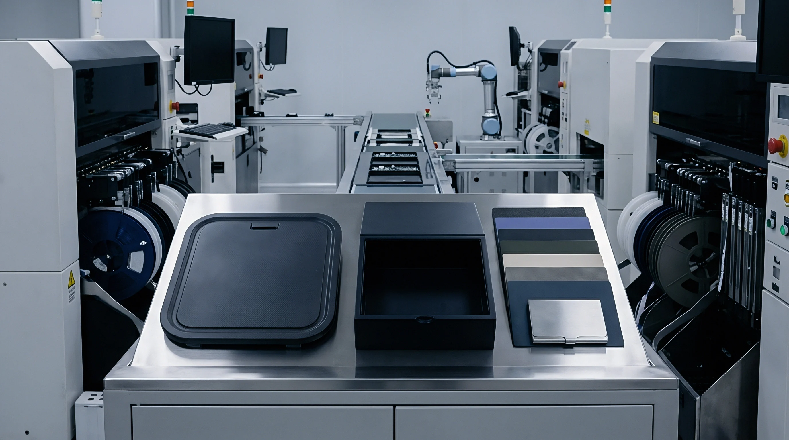
Thermal management during high-density surface mount assembly dictates initial intermetallic thickness and atomic diffusion rates. High peak temperatures and extended time above liquidus drive excessive growth of the primary epsilon-phase layer, increasing the vacancy flux entering the copper pad. Setting thermal parameters requires balancing full solder wetting against overgrowth of the intermetallic layer.
Reflow profiles for complex, high-density assemblies must keep peak temperatures within narrow windows. Exceeding 245°C on SAC305 assemblies accelerates copper dissolution into liquid solder, generating a thick, brittle eta-phase layer. Restricting time above liquidus limits the initial solid-state diffusion window when early vacancies condense.
| Profile Parameter | Standard Window | High-Density Limit | Microstructural Consequence |
|---|---|---|---|
| Peak Temperature | 240°C – 250°C | 235°C – 242°C | Elevated temperatures double copper dissolution rates into solder. |
| Time Above Liquidus | 60 – 90 Seconds | 45 – 60 Seconds | Extended duration thickens initial epsilon-phase layer beyond 1.2 µm. |
| Cooling Rate | 2.0°C/s – 4.0°C/s | 3.0°C/s – 5.0°C/s | Slow cooling allows vacancy migration and early void growth. |
| Preheat Ramp Rate | 1.0°C/s – 2.0°C/s | 1.5°C/s – 2.0°C/s | Excessive preheat time increases thermal exposure of underlying pads. |
Establishing tight profile controls across a dense assembly requires a systematic adjustment routine on the SMT line.
- Calibrate multi-channel thermocouple boards attached to high-thermal-mass components and fine-pitch packages to identify maximum thermal gradients.
- Adjust conveyor speed to lock time above liquidus strictly between 45 and 60 seconds across all measured joint locations.
- Cap maximum peak solder temperature at 240°C to minimize liquid-solid interfacial copper dissolution rates.
- Establish forced-convection cooling zone parameters to maintain a post-reflow cooling rate between 3.0°C and 5.0°C per second.
Allowing reflow peak temperatures to drift up by as little as 8°C increases total intermetallic volume by twenty-five percent, triggering early microvoid nucleation that cuts field operating life in half.

Drop
Mechanical stress exposes structural weaknesses created by interfacial microvoids. High-density assemblies in handheld devices, automotive control modules, and aerospace electronics face severe drop-impact, vibration, and thermal flexure. At rapid strain rates, bulk SAC solder work-hardens, transferring load straight to the thin, brittle intermetallic interface.
When microvoids occupy more than fifteen percent of the planar area along the copper to Cu3Sn junction, the effective load-bearing area drops proportionally. Stress fields concentrate at the edges of individual voids, initiating micro-cracks under drop shock. Cracks propagate rapidly along the coalesced void plane, causing complete open-circuit failure.

How Does Thermal Aging Accelerate Brittle Interfacial Fracture?
Elevated operating temperatures drive solid-state diffusion throughout months of field deployment. As mobile vacancies migrate toward existing void nuclei, small isolated voids merge into wide planar channels. High-speed ball pull and cold bump shear testing per IPC-TM-650 Method 2.4.53 track this failure mode shift, where solder joints transition from ductile bulk shearing (Mode 1) to clean, brittle cleavage along the copper interface (Mode 4 or Mode 5).
IPC-6012 Class 3 performance requirements mandate cross-sectional evaluation of plated copper purity to prevent brittle interfacial separation under thermal stress.
Microvoids discovered during failure analysis are often attributed to mechanical overload during assembly handling or drop testing. This explanation ignores the metallurgical reality that mechanical stress merely opens pre-existing planes of weakness created by impurity-driven vacancy condensation. High strain rate testing validates whether pad metallurgy possesses adequate fracture energy resistance.
Foil
Substrate pad metallization choices directly dictate diffusion mechanics during reflow. Direct electrodeposited copper with Organic Solderability Preservatives is the most common and cost-effective finish, yet it carries the highest risk of Kirkendall voiding if copper purity goes unmanaged. Alternative surface finishes insert barrier layers or modify interfacial reaction chemistry to prevent direct tin-copper contact during reflow.
Electroless Nickel Immersion Gold eliminates direct copper diffusion by placing a nickel-phosphorus alloy barrier over the copper pad. Solder reacts with the nickel to form a Ni3Sn4 intermetallic layer, preventing Kirkendall microvoid formation at the copper interface. However, nickel finishes introduce their own failure modes ~ including hyper-corrosion of the nickel layer, known as black pad defect, if bath chemistry controls slip during plating.
| Surface Finish | Interfacial Reaction | Kirkendall Risk Level | Primary Failure Mode | Cost Delta per m² |
|---|---|---|---|---|
| OSP on Direct Cu | Cu3Sn / Cu6Sn5 formation | High (Impurity dependent) | Interfacial Kirkendall Cleavage | Baseline |
| ENIG | Ni3Sn4 formation | Negligible at Cu Interface | Hyper-Corrosion / Black Pad | +$18.00 to +$25.00 |
| ENEPIG | (Pd,Ni)Sn4 formation | Zero at Cu Interface | Brittle Pd-Rich Intermetallic | +$35.00 to +$48.00 |
| Immersion Silver | Cu3Sn / Cu6Sn5 formation | Moderate to High | Silver Migration / Voiding | +$8.00 to +$12.00 |
Selecting substrate surface finishes requires precise criteria to protect high-reliability designs against interfacial cracking.
- Impurity cap enforcement requires specifying maximum sulfur limits below 10 parts per million in raw electrodeposited copper foil procurement contracts.
- Finish barrier layer selection specifies ENEPIG for mission-critical assemblies to eliminate direct copper diffusion while avoiding black pad risks.
- Thermal budget accounting limits total allowable reflow and rework passes based on the underlying pad metallization chemistry.
Consider a production run of 50,000 automotive control units manufactured in Guangdong. Baseline OSP copper substrate costs $42.00 per square meter. Upgrading to high-purity copper foil with Glow Discharge Mass Spectrometry certification for sulfur under 10 ppm adds $3.50 per square meter.
If uncertified copper yields a 1.2% field return rate from drop-impact brittle fractures, total warranty recovery, freight, and board replacement costs reach $185,000. Purchasing certified low-sulfur substrate adds $4,375 in total material cost across the build, eliminating $180,625 in unrecoverable field liability.
Raw circuit board substrates ordered without chemical impurity caps transfer the cost of plating bath maintenance directly to the assembly line scrap report.
Substrate supply contracts carrying IPC-4552 specifications for plating thickness hold vendors legally responsible for interfacial failures resulting from out-of-spec chemical contamination.

Lien
Preventing interfacial fracture across cross-border supply chains requires commercial mechanisms that enforce technical standards on the factory floor. The distance between design teams and assembly plants in Kunshan or Shenzhen often leads to miscommunication over plating quality expectations. Quality agreements must translate metallurgical requirements into binding inspection routines, holding funds until verification passes established thresholds.
Incoming circuit board lots undergo mandatory quarantine upon arrival at the assembly plant. Receiving inspection protocols run thermal stress simulations by floating raw board samples three times on a 260°C solder bath per IPC-TM-650 Method 2.4.13. Inspectors section sample pads and analyze the copper-intermetallic interface using scanning electron microscopy or high-resolution optical metrology to quantify void planar area fractions before mounting components.
Commercial contracts retain fifteen percent of total purchase order value in a quality holding fund, payable sixty days after SMT assembly completion. If post-reflow microsectioning reveals a Kirkendall microvoid linear density exceeding 10 voids per 100 micrometers, the lot is rejected. The contract obligates the PCB manufacturer to pay full replacement costs for scrapped active components mounted on defective boards, shifting financial liability back to the substrate supplier.
Stationing a resident quality engineer at the circuit board plating plant costs approximately $4,500 per month. A single rejected SMT assembly batch containing high-value microprocessors easily exceeds $120,000 in unrecoverable scrap. Continuous oversight of bath maintenance, additive extraction, and low-sulfur foil procurement proves far less expensive than absorbing the commercial losses of field failures.